High-speed digital electronics create a lot of electromagnetic noise. Without mitigation, this high-frequency interference bleeds into sensitive analog lines or radiates outward, causing your device to spectacularly fail FCC emissions testing.
The primary weapon against this interference is the ferrite bead. Understanding its schematic symbol and placement dictates whether your circuit operates cleanly or drowns in its own noise.
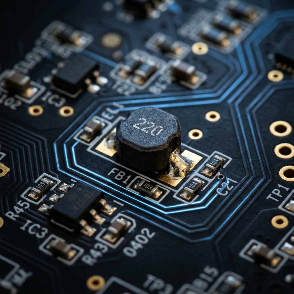
1. Visualizing the Ferrite Bead Symbol
A ferrite bead operates inherently like a heavily lossy inductor. Because of this, its schematic symbol is closely related to the standard inductor symbol, but tailored to emphasize its specific role.
graph LR
    A[Inductor Basis] --> B(Standard Inductor Symbol)
    A --> C(Rectangle Over Wire)
    B -.-> D(Addition of a dashed line or solid bar)
    D --> E[IEEE Ferrite Symbol]
    C --> F[IEC Ferrite Symbol]

    style E fill:#0f172a,stroke:#3b82f6
style F fill:#0f172a,stroke:#10b981| Trait | IEEE/ANSI Standard | IEC Standard | Notes |
|---|---|---|---|
| Shape | Series of semi-circles with a bar/box | A solid rectangular block | Functionally identical in outcome |
| Designator Prefix | FB | FB or L | Using FB is highly recommended to prevent confusion with power inductors |
| Measurement Unit | Ohms (Ω) at specific MHz | Ohms (Ω) at specific MHz | Unlike inductors measured in Henries (H) |
Crucial Distinction: Never rate a ferrite bead by inductance. Ferrite beads are specified by their impedance (in Ohms) at a specific frequency (typically 100 MHz).
2. Core Operational Mechanics
Why use a ferrite bead instead of a standard inductor?
- An inductor stores energy and returns it to the circuit. It is highly reactive and preserves energy.
- A ferrite bead is actively designed to be lossy. At high frequencies, it behaves like a resistor, converting unwanted high-frequency noise directly into heat.
| Frequency Range | Ferrite Bead Behavior | Result on Circuit |
|---|---|---|
| Low Frequency / DC | Under 1 MHz | Acts like a simple wire (~0 Ω). DC power passes through freely. |
| Resonant Frequency | Highly Reactive | Stores energy briefly. |
| High Frequency | Over 50 MHz+ | Acts like a high-value resistor. Blocks and dissipates RF noise as heat. |
3. Best Practices for Schematic Placement
Properly utilizing the FB symbol requires strategic placement. Slapping ferrite beads randomly on a schematic can actually worsen ringing and resonance.
Decoupling Power Supplies (Pi-Filters)
The absolute most common use for an FB symbol is isolating dirty digital power from clean analog power.
flowchart LR
    VCC[Main VCC 5V] -- Dirty Digital Noise --> FB1[Ferrite Bead]
    FB1 -- Cleaned Analog Power --> AVCC[Analog VCC]

    FB1 --- C1[Decoupling Cap]
    C1 --- GND[Ground]

    style VCC stroke:#ef4444
    style AVCC stroke:#10b981
In the configuration above (part of a Pi-Filter), the ferrite bead blocks high-frequency transients from entering the AVCC line, while the capacitor shunts any remaining ripple down to ground.
Data Line EMI Suppression
When routing long USB data cables or HDMI traces, FB symbols are often placed in series near the connector. This ensures that the long, physically exposed wire does not act as an antenna and radiate CPU noise across the room.
To add a ferrite bead to your next schematic, open the Circuit Diagram Editor, search for “Ferrite,” and specify your impedance rating!