Before the massive proliferation of MOSFETs, the JFET (Junction Field-Effect Transistor) was the king of high input impedance amplification. While not used as frequently in modern digital logic, they remain indispensable artifacts in high-fidelity audio preamplifiers, sensitive instrumentation, and RF circuitry.
Understanding the JFET schematic symbol is essential for anyone delving into discrete analog circuit design.
1. Anatomy of the JFET Symbol
Unlike Bipolar Junction Transistors (BJTs) which are current-controlled devices, a JFET is a voltage-controlled device. The schematic symbol attempts to visually represent the physical construction of its internal semiconductor channel.
mindmap
  root((JFET Pins))
    Gate
      Controls electron flow
      High Input Impedance
      Analogous to a valve
    Drain
      Current enters (N-Channel)
    Source
      Current exits (N-Channel)
The symbol consists of a straight vertical line representing the channel, with two horizontal lines hooking into it (the Drain and Source). A third perpendicular line forms the Gate, complete with an arrow that dictates the semiconductor polarity.
N-Channel vs. P-Channel JFETs
Just like BJTs have NPN and PNP, JFETs come in two distinct flavors.
| Characteristic | N-Channel JFET | P-Channel JFET |
|---|---|---|
| Symbol Arrow | Points IN toward the channel line | Points OUT away from the channel |
| Majority Carriers | Electrons | Holes |
| Vgs for Pinch-Off | Negative Voltage (e.g., -5V) | Positive Voltage (e.g., +5V) |
| Typical Operation | Normally ON -> Apply negative voltage array to turn OFF | Normally ON -> Apply positive voltage array to turn OFF |
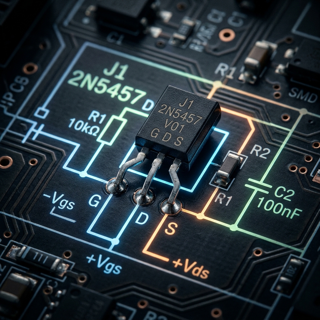
Memory Trick: “Pointing IN” means N-Channel. Look at the arrow on the Gate. If it points inward to the line, you are dealing with an N-Channel JFET (like the popular 2N5457).
2. Operation: The Depletion Mode
One of the most defining characteristics of a JFET is that it is a Depletion Mode device. This vastly affects how you design schematics around them.
- MOSFETs (Enhancement Mode): Are normally OFF. You must apply a voltage to the gate to turn them ON.
- JFETs (Depletion Mode): Are normally ON. With 0 Volts at the gate, maximum current flows from Drain to Source. You must apply a reverse bias voltage (negative for N-Channel) to expand the depletion region and literally “pinch off” the flow of electrons, turning the device OFF.
flowchart LR
    VGS[V_GS = 0V] --> I1[Maximum Drain Current flows]
    VGS2[V_GS = -2V] --> I2[Current is restricted]
    VGS3[V_GS = -5V] --> I3[Pinch-Off reached. Circuit is OFF]

    style VGS fill:#1e293b,stroke:#f59e0b
    style VGS3 fill:#1e293b,stroke:#ef4444
3. Typical Schematic Applications
Because the Gate of a JFET is reverse-biased during operation, essentially zero current flows into it. This yields an astronomically high input impedance (often measured in hundreds of Megaohms).
| Circuit Application | Why JFETs Are Chosen | Schematic Clues |
|---|---|---|
| Audio Preamplifiers | Extremely low noise and massive input impedance prevents loading of sensitive electric guitar pickups. | Often seen acting as a Source Follower buffer stage. |
| Analog Switches | Because they are purely voltage controlled with no gate current, they inject zero switching transients into the signal path. | Placed in series with an analog signal passing through the drain-source channel. |
| Constant Current Sources | A JFET behaves natively as a constant current sink when the gate is tied directly to the source. | Gate terminal wired directly around to the Source terminal. |
When diagramming these specialized analog circuits, precision is key. Ensure your Gate arrow orientation is correct to prevent manufacturing failures. Use the curated discrete semiconductor library in Circuit Diagram Maker to place standard N-Channel and P-Channel JFET symbols accurately on your next canvas.